1. Introduction
The development of wireless communications imposes more and more stringent requirements on the phase noise. The adequate phase noise computer modeling and simulation allow the investigation, prediction and minimization of this important characteristic at the design stage.
In wireless transceivers, a significant part of the power is consumed by the VCO (Voltage Controlled Oscillator). VCOs are implemented in silicon-based technologies which are mainly realized as differential cross-coupled topologies due to the poor substrate isolation properties of silicon based technologies. Their efficiency is low because in addition to the oscillator core, an output buffer is needed [1-3]. Phase and frequency fluctuations have therefore been the subject of numerous studies [4-9].
Since the (low frequency) noise sources present in the circuit play a significant role in generating the phase noise, MOS oscillators are especially prone to higher phase noise because of the notoriously poor 1/f noise performance. Therefore, it is essential to design them carefully in order to implement better RF CMOS integrated circuit (ICs) and to push the performance limits of CMOS implementations.
Phase noise in RF oscillators is an important item in the design of integrated transceivers. As a result, different phase noise theories have emerged. Several papers addressing phase noise have been published [5,10-14]. Recently, Hajimiri and Lee [10] have proposed a time variant model (LTV) based on the so-called Impulse Sensitivity Function (ISF) to predict phase noise. This technique provides insight into the design of oscillator. The ISF function characterizes only the stationary results of a perturbation.
In this work, we want to investigate some phase noise phenomena. We will apply the theory described by Hajimiri and Lee in 1998, which makes use of the ISF function.
The paper is organized as follows. In Section 2, we present the double gate transistor structure and the Poisson-Schrodinger model is considered. In Section 3, we present the static characteristics (DC) for the DGMOS and we point the reduction of short channel effect (SCE) in this structure. Section 4 presents a Colpitts oscillator using a mixed-mode simulation, which is carried out using the DESSIS tool in the ISE-TCAD [15]. A brief outline of the phase noise model will be given in Section 5. Finally, Section 6 presents the method to calculate Impulse Sensitivity Function and Section 7 extends and concludes this study.
2. Presentation Device
The geometry that we consider is bidimensional. Figure 1 shows the DG MOSFET device used in this paper with the following parameters: channel length LG = 10 nm, oxide thickness TOX = 1.5 nm, silicon thickness TSi = 1.5 nm; source/drain length LSD = 5 nm. The source and drain regions are doped ND = 1020 cm−3, the channel is undoped NA = 10−10 cm−3 (Figure 1). The threshold voltage of the DG MOSFET is adjusted to be 0.15 V using a gate work function equals 4.25 eV. The voltages VGS applied to the two gates are identical. All calculations were done at the temperature 300 K.
This device was simulated with a 2D solution to Poisson equation coupled to a 1D Schrödinger equation. Usually, 2D Poisson equation describes electrostatic transport and 1D Schrodinger equation is used to handle the quantum transport. The coupling of Poisson and Schrödinger equations is necessary when the oxide thickness is decrease and the thickness of the channel takes values close to the wavelength of the electrons. This approach is justified by several results presented in the literature [16,17].
The Poisson (1) and Schrodinger (2) equations are given by the following equations:
 (1)
(1)
 (2)
(2)
where: V(x,y) is the electrostatic potential; ρ(x,y) is the charge density; ε is the permittivity of the dielectric material constant; m* is the electron effective mass, q is the electron charge, h is the Planck’s constant and ψ(y) is the wave function corresponding to the eigenvalue E.
We clearly see that the Equations (1) and (2) are coupled. It is therefore self consistency in their resolution. We can illustrate the self consistent system by the following one:
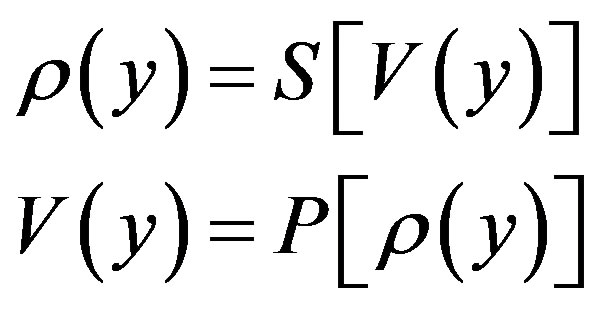

Figure 1. Schematic of the double gate MOS transistor.
where, the functions S[V(y)] and P[ρ(y)] represent the Schrödinger and Poisson equations.
The Poisson and Schrodinger equations are discretized using the finite difference method:
For the Poisson’s equation:
 (3)
(3)
The discrete Poisson equation is nonlinear, and therefore written as:
 (4)
(4)
where: F(Vi) is the Poisson equation functional.
The potential V, solution of Equation (4) can be written as: V = Vi + ΔVi.
For a limited development in Taylor series of a first order, we can write:
 (5)
(5)
where: J is the Jacobian system matrix (4), which equals to the derivative of the Poisson equation functional.
 (6)
(6)
From the expression (5) we obtain:
 (7)
(7)
For the Schrödinger equation:
 (8)
(8)
Discretized Schrödinger equation can be written in a matrix form:
 (9)
(9)
where: H is the Hamiltonian system defining by:
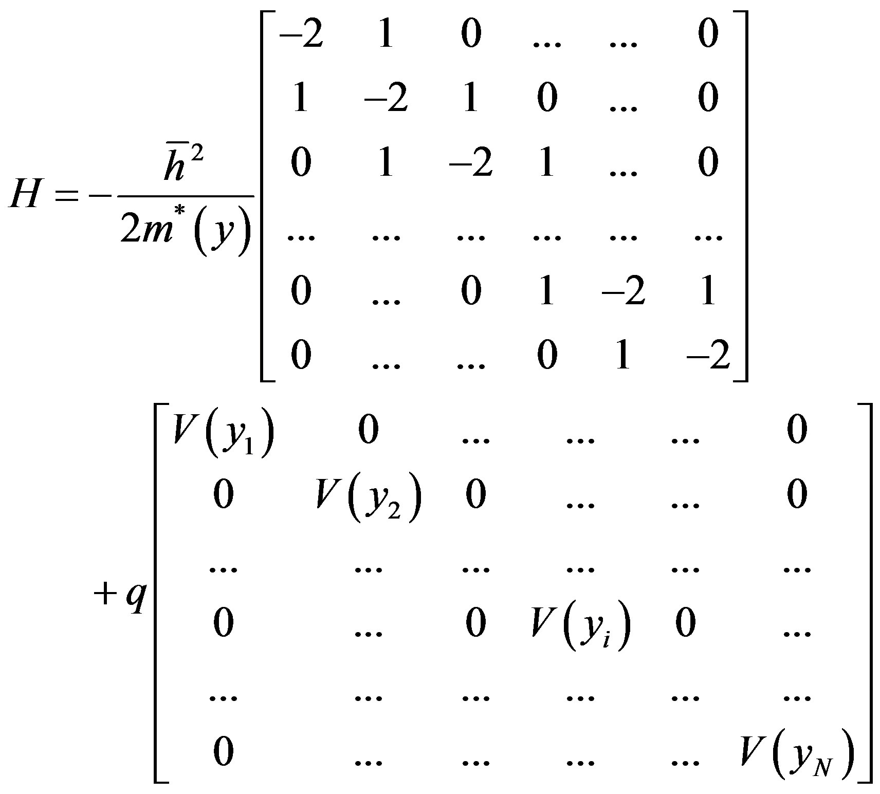
For solving the Schrödinger equation, one must know the electrostatic potential V(x,y) and to solve the Poisson equation, we must know the carrier concentration or charge density ρ(x,y). There is therefore self consistency between the resolutions of the 2D Poisson and the 1D Schrödinger equations.
3. DC Characteristics
The static characteristic of the considered DGMOS is obtained by self-consistent Poisson-Schrodinger system. Figure 2 presents the potential energy obtained: VDS = 0.6 V, VGS = 0.6 V bias voltages. The potential energy barrier between source and channel is pointed.
The evolution of the potential energy of double gate structure for different gate voltages VG is presented Figure 3. We observe that the potential barrier decrease with the increasing of the gate voltage. At low gate voltage, the potential barrier of the channel allowed the passage of electrons from the source to the drain. In this case, the transistor is blocked. By contrast for higher values of gate voltage the potential barrier decreases and the electrons can pass from the source to the drain and a current

Figure 2. Potential energy of DGMOS.

Figure 3. Potential energy along the channel vs gate bias.
drain IDS is then obtained.
Figure 4 represent IDS (VGS) characteristics for different channel lengths. It can be observed that when channel length (LG) decrease, drain current (IDS) increase also IOFF (off-current) increase too; as well as lead to a decrease of the threshold voltage dramatically. In order to have an acceptable threshold voltage, we study the influence of the gate work function (Figure 5).
On conclude that for a nanometric length of channel, and in order to optimise the threshold voltage, the solution is to choose a gate metal with a high value of work function.
4. Colpitts Oscillator Build around the Considered DGMOS
A mixed-mode analysis involve, applying a 2D Poisson-

Figure 4. Influence of the channel length on the current drain with VDS = 0.6 V and Φm = 4.25 eV.

Figure 5. Influence of the gate work function on the current drain for different gate voltages; with VDS = 0.6 V and LG = 10 nm.
Schrodinger model to the device, whereas the rest of the circuit used is governed by Kirchhoff’s laws (Figure 6(a)). We present in Figure 6(b) a Colpitts oscillator typical case: T = 335.8 ps (period). We use the same values used in [18], except in the component of oscillator Colpitts, we changed the values for obtaining the carrier frequency very near 3 GHz. Mixed mode simulations were carried out using the DESSIS tool in the ISE-TCAD [15].
4.1. The Noise Phase Model
Although all components of a circuit create noise, the major source of noise in an oscillator is the active device. The noise sources in any oscillator circuit ultimately combine to form amplitude noise and phase noise. The phase noise is usually characterized in the frequency
 (a)
(a) (b)
(b)
Figure 6. (a) Colpitts oscillator of our simulation; (b) a typical response of the DGMOSFET oscillator (mixed-mode simulation).
domain. For an ideal oscillator, the output can be expressed as Vout(t) = V0cos[ω0t + Φ0], where the amplitude V0, the frequency ω0, and the phase reference Φ0 are constants. The phase noise is given by the following [10]:
 (10)
(10)
where Psideband(ω0 + Δω, 1 Hz) represents the single sideband power of the Δω frequency offset, and Pcarrier is the total power. Therefore, the unit for phase noise by definition is dB/Hz, which reads decibel with respect to carrier per Hertz (Figure 7).
The phase noise models describe the phase noise generation mechanism in oscillators. There are, at present, two models of phase noise oscillator output: Leeson’s Model and Hajimiri’s one. In order to increase the accuracy of the phase noise predictions a more sophisticated theory is needed Hajimiri’s model.
4.2. Linear Time-Variant (LTV) Phase Noise Model: Hajimiri’s Model
Hajimiri’s model is based on the time-varying properties of the oscillator current waveform and the resultant implications on the phase noise production.
The main idea of Hajimiri’s phase noise model is to characterize the phase noise of an oscillator by its phase impulse response. It implies that a given voltage or current impulse cause phase shift. So the phase noise can be characterized by an impulse response [10] as:
 (11)
(11)
where u(t – τ) is the unit step function, qmax, the maximum charge displacement, Γ(ω0τ) is the impulse sensitivity function (ISF). This later is periodic; it can be expressed as a Fourier series:
 (12)
(12)

Figure 7. Phase noise with respect to carrier power per unit bandwidth.
where C0 is the flicker noise conversion factor and Cn is the white noise conversion factor. The phase noise predicted using Hajimiri’s model is [10]:
 (13)
(13)
where Γrms is the root mean square value of the ISF and  the power spectral density of the white noise source. The LTV phase noise model can predict the phase noise, but it is difficult to define the ISF function by simulation.
5. Determination of the ISF Function
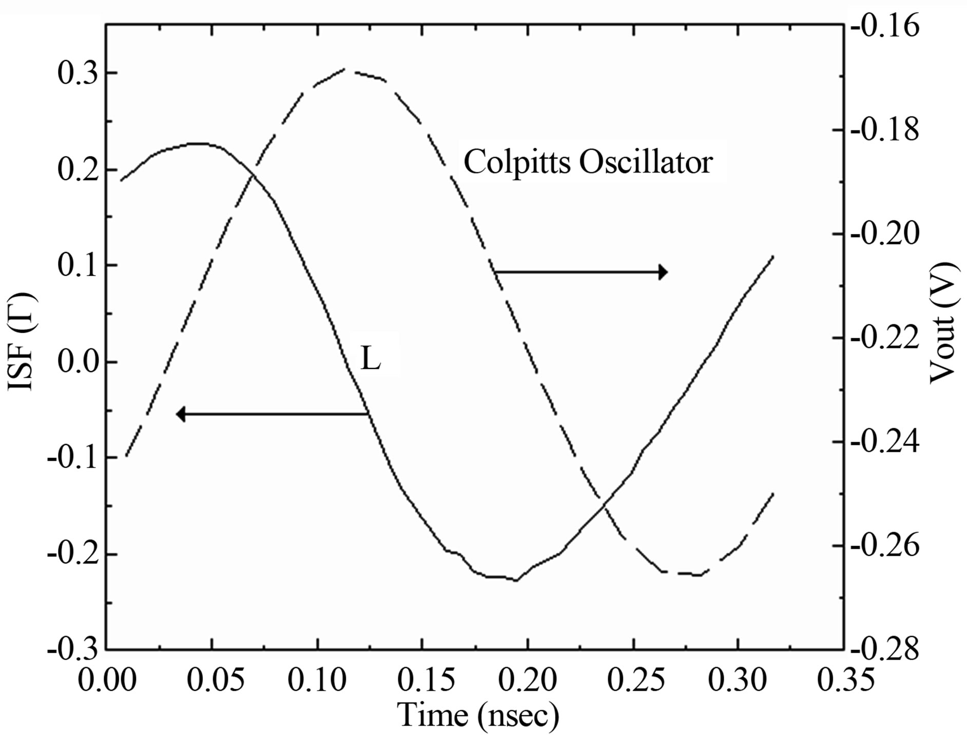
In this section, we use the linear time-variant model described by Hajimiri to analyze the Colpitts oscillator sensitivity. The method is based on the ISF calculation; this function is used to study the sensitivity of the elements (L, C1, and C2) of the Colpitts oscillator to a current disturbance.
For determining the ISF, we inject a pulse i(t) at time τ of period T and simulate the oscillator response for a few periods after the injection. By measuring the deviation ∆t of the moment of zero crossing, we can measure the phase difference ΔΦ = 2πΔt/T, produced by the injection (Figure 8). We change the moment of injection τ to cover a full period and repeats the procedure [19].
The source i(t) is injected into the node of the oscillator output. In our measurement, the setting time of injection is increased in steps of 0.00674 ns to cover a period T0 = 1/f0 = 1/2.97 GHz 0.3358 ns. The total number of points of the ISF is 50 points per period.
The main interest of this study is to obtain the sensitivity of the elements (L, C1 and C2) of the Colpitts oscillator (Figure 9). We can observe that the ISF function attained its maximum when the oscillant signal pass by zero.
6. Theoretical Extension on Oscillator Phase Noise
Now, we would like to extend the discussion to any value

Figure 8. Injection of an impulse at t = τ0.
 (a)
(a) (b)
(b) (c)
(c)
Figure 9. The impulse sensitivity functions versus the oscillation period.
of the Φ phase (Φ Î [0, 2π]), not only for a small charge injection.
If we consider a parasitic pulse injection (a “dirac”) at τ time, the global output voltage of an oscillator can be considered as the superposition of the permanent voltage and the response to the parasitic injection, because any time or phase shifted solution remains a solution of the harmonic oscillator:
 (14)
(14)
 (14bis)
With:
VT: total output voltage Vs: output voltage of the free oscillator (without parasitic pulse)
C: global capacity of the Colpitts tank, C1C2/(C1 + C2), (see Figure 6).
This equation can be reformulated as:
 (15)
(15)
With
 (16)
(16)
 (16bis)
*note: we get directly the ISF, by deriving (16bis):
 (17)
(17)
Now, from these general formulas, and assuming a limited expansion of φ, we obtain:
 (18)
(18)
If we consider only the first order, we get:
 (19)
(19)
If we compare this latter formula to [10, appendices], we find the well known result:
Γ = –sin(ω0t)-see Equation (11), with qmax = CV0; this result is valid, but for q very small. Note that a small signal analysis cannot yield any information on the amplitude of the oscillation, as this is determined by the nonlinearities of the system. In a real circuit, the frequency of oscillation depends on the transistor junction capacitances (that can be handled by our mixed mode simulations, anymore).
We represent on the Figure 10, φ versus q, extracted from mixed-mode simulations, and compare it to the “arctan” analytical solution of equation16 bis, where C is given:
By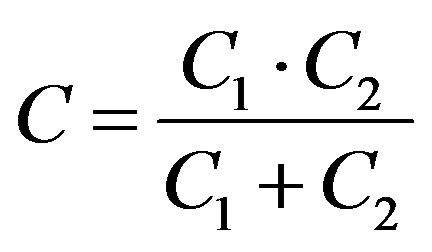 . In this typical case, we have from the “mixed-mode” CV0 = 100 fc, in very good accordance with the “arctan” fit of equation 16 bis, considering also the graph asymmetry (shift) along the y axis. We have chosen, for this characteristic calculation, an angle very near of 90˚, for a high φ magnitude (not exactly 90˚, to “observe” the influence of the denominator of equation (22 bis), i.e.: 81˚ (90˚ - 10% of 90˚).

Figure 10. Phase shift (output of transistor) versus injected charges (mixed mode compared to our analytical model).
Up to our knowledge, it is the first time that such comparisons are presented. Their interest is twofold: our “microscopic” simulations seem validated by our analytical formulations, and we do not need to stay in the linear domain, like in the standard ISF theory–see, for instance: ([10], Figure 6)–where only a very limited domain of φ versus q is consider. In fact, to have some coherent results, using SPICE simulations, the effective charge injected due to actual noise and interference sources is supposed to be several orders of magnitude smaller than the amounts of charges injected, which is too restrictive, in actual circuits.
According to the Equations (16) and (16bis), phase or/and amplitude can change after the perturbation. We represent on Figure 11 some mixed-mode simulations when applying a pulse on VDD .Our observations are:
- At zero crossing For  (
( , or τ = T/4 or 3T/4):
For zero crossing falling (τ = T/4): φ = –φmax; For zero crossing rising (τ = 3T/4): φ = φmax.
 (20)
(20)
This is quite negligible if q is small (q/C = V0: our case).
- At the peaks For φ = φmin = 0: ω0τ = π or 2π, or τ = T/2 or T):
 (21)
(21)
That mean for ω0τ = 2π
 (22)
(22)
and ω0τ = π: (22 bis)
Our “raw” simulations (q < 0-current pulse negative) show these results (cf. Figure 11), with some good numerical accuracy; if we consider the relation with typically ΔV =1 to 5 mV, that implies that abs(q) = 5 to 15 fc, which is well in the linear domain of φ versus q .
To go further, an interesting question is: how to calculate phase noise, when Dirac pulses are applied?
The φ(τ)/ω fluctuations are to the phase noise origin, depending on the noise sources (e.g. process induced traps for the devices, jitter noise).
If we are interested by time fluctuations, we can study the following expression:
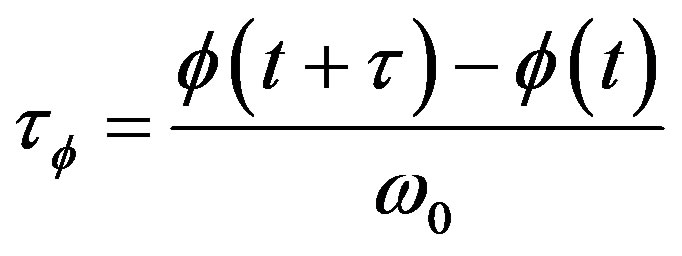 (23)
(23)
Taking the square of its RMS value:
 (24)
(24)
If now, we say that this process is a second order stationary one, the RMS value does not depend on time, i.e.
 .
.
The second term in the right side-Equation (24)-is the so called correlation function: Cφ(τ).
Then Equation (24) is reduced to:
 (25)
(25)
Take back the parasitic waveform which comes from a capacitive charge injection, at f0 frequency, as treated above; we have (for weak values of φ; otherwise: take Equation (18).
 (26)
(26)
 (27)
(27)
And  (27bis)
Or  (28)
(28)
This gives the associated noise power density:
 (29)
(29)
The last goal is to calculate the oscillator power spectral density output (PSD), via the autocorrelation output voltage:
 (30)
(30)
(FT: Fourier Transform)
It is easy to verify that the variance satisfy the relations:
 (31)
(31)
With these conditions and the fact that φ(t) varies slowly over time, Equation (30) can be approximated as:
 (32)
(32)
With φ2 is given by (28).
Then, the Equation (32) can be rewritten:
 (33)
(33)
Find the Fourier Transform in Equation (33) comes down to find the Fourier transform of  i.e.:
i.e.:
 (34)
(34)
This general formula (numerical solution), can be reduced, for the specific case where q = CV0; Equation (33) can be rewritten:
 (35)
(35)
That gives:
 (36)
(36)
7. Conclusions
In this paper, the analysis of a Colpitts oscillator designed in a nanometer CMOS technology is presented. Firstly, we have analyzed the drain current in DGMOS devices; we see that if the gate lengths or work functions are increased, the drain current is decreasing. The future trends will analyse the Double Gate transistor with Highk gate dielectric.
Secondly, we go further on phase noise theory of such oscillator, starting with mixed mode analysis of a LCtype oscillator; we derive some analytical solutions for the phase noise, through a new lecture of the impulse sensitivity function (ISF). Our first numerical simulation raw results are very consistent with such a numerical model. So, we have been invited to study more in-depth of the ISF, and try to extend its efficiency.
The future trends will lead to apply these later theoretical insights to a resonant tunnelling nano-device, not only on a first order approach, but also on a noise point of view.
Acknowledgements
This work is supported by UPM (Union pour la méditéranée)