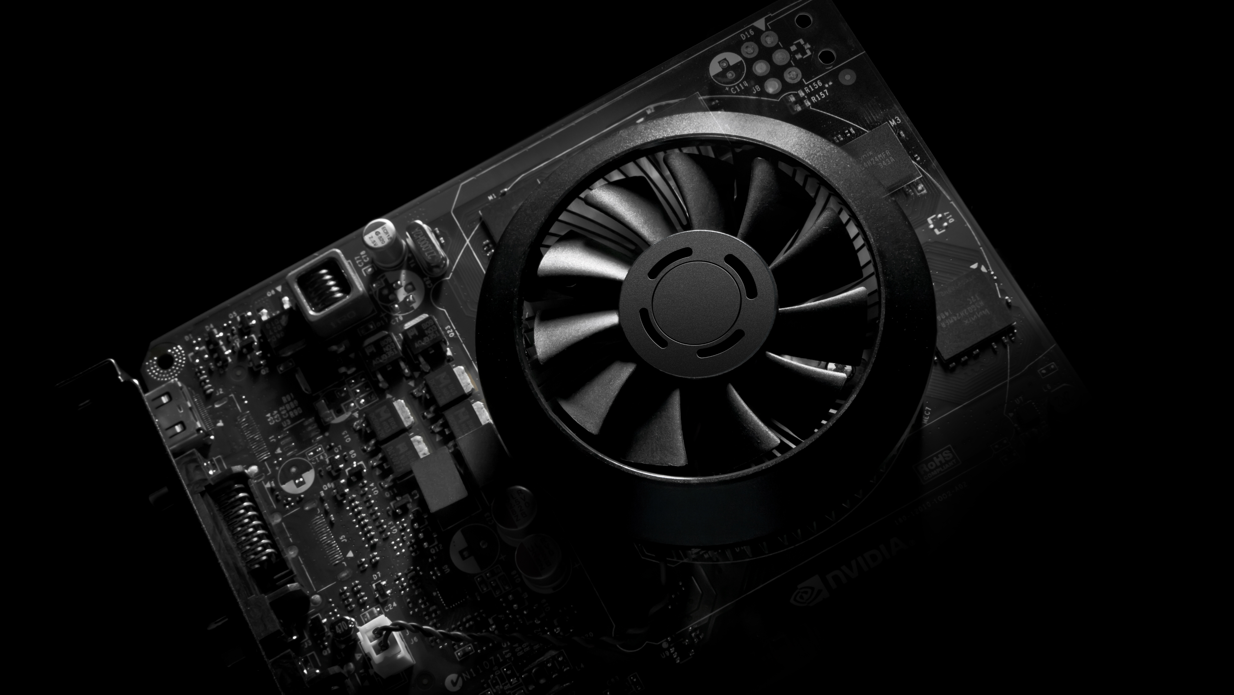
Nvidia announces a new generation of graphics with Maxwell
Unleashes the GTX 750 Ti

Today Nvidia released its first product using the GM107 Maxwell Architecture, the Geforce GTX 750 TI which will sell for £115 ($149, about AU$165).
Nvidia claims that the card can match the performance of its flagship GPU from four years ago, the GeForce GTX 480, but with only a 60W TDP, that's a fourth of the power dissipated.
However, the GTX 750 TI is less interesting than the architecture. Maxwell design is mostly about power efficiency per watt consumed with the GPU targeted for use in power-limited environments like notebooks and small form factor PCs.
The graphics market is becoming more vital as the likes of Steam want to serve up games on lower spec machines.
At the heart of Maxwell is an all-new design for the streaming multiprocessor that improves performance per watt. This is an improvement on Kepler and was managed through improvements to control logic partitioning, workload balancing, clock-gating granularity, compiler-based scheduling and number of instructions issued per clock cycle.
Nvidia has also increased the number of SMs to five, compared to two in GK107. Maxwell also has a larger L2 cache design of 2048KB instead of 256KB. With more cache on the chip, fewer requests to the graphics card DRAM are needed.
Maxwell power
On the graphics side, Maxwell has a similar structure to Kepler. It also uses several streaming multiprocessor units within a Graphics Processing Cluster. Each streaming multiprocessor includes a polymorph engine and texture units, while each GPC includes a raster engine.
Are you a pro? Subscribe to our newsletter
Sign up to the TechRadar Pro newsletter to get all the top news, opinion, features and guidance your business needs to succeed!
The GM107 GPU contains one GPC, five Maxwell streaming multiprocessors and two 64-bit memory controllers which means 128-bit in total.
Nvidia claims that Maxwell delivers 35% more performance per Cuda core on shader-limited workloads and needed some heavy work on scheduler architecture. Some algorithms had to be rewritten to avoid stalls and cut power loss.
Each SM is partitioned into four separate processing blocks, each with its own instruction buffer, scheduler and 32 Cuda cores. This partitioning simplifies the design and scheduling logic, saving area and power, and reduces latency.
On the video front, Maxwell has an improved NVENC block that promises a faster encode speed of 6-8X real-time for H.264 and 8-10X faster decode, and thanks to a new local decoder cache, higher memory efficiency per stream for video decoding, resulting in lower power for video decode.
Maxwell features a new GC5 power state that has been tailored to reduce the GPU's power consumption for light workload cases like video playback.
Most Popular

