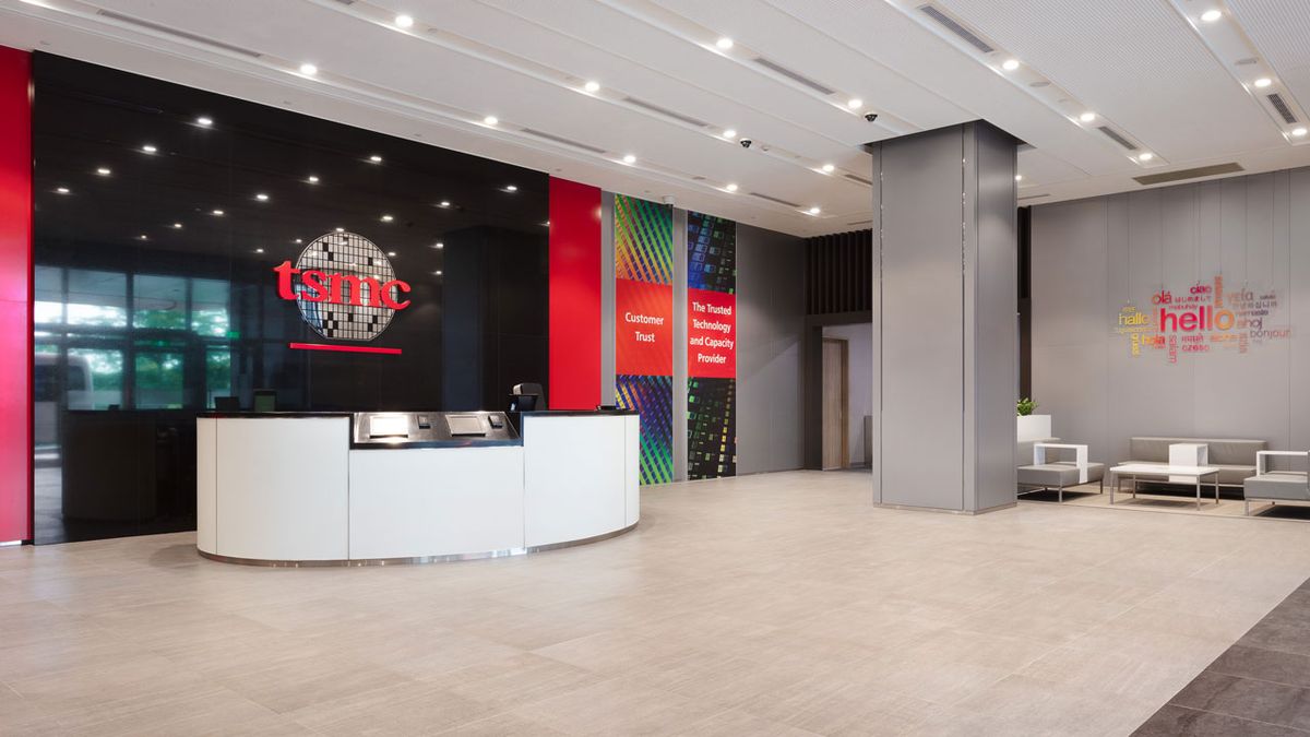
TSMC's first new overseas fab in years begins to make chips — JASM coming online
Japan gets 16nm process technology.

TSMC has commenced mass production at its fab in Kumamoto, Japan, marking a significant milestone in advanced chip manufacturing for the country and the first step in its major expansion overseas, reports Nikkei. The plant, operated by Japan Advanced Semiconductor Manufacturing (JASM), produces chips using a variety of process technologies for TSMC's major customers in Japan, reports DigiTimes.
As TSMC's Kumamoto fab kicks off operations, this marks the first time logic chips featuring FinFET transistors have been made in the Land of the Rising Sun. TSMC's new fab near Kumamoto on Kyushu Island can process up to 55,000 300-mm wafer starts per month (WSPM) using TSMC's 40 nm, 28 nm, 22 nm, 16 nm, and 12 nm-class process technologies. Several variants of N28 are meant to address automotive and mature applications, whereas the 22ULP process aims at ultra-low-power applications. As for N16 and N12 production nodes, they are meant to address the demands of more performance-hungry applications that can take advantage of FinFET transistors.
While 16nm-28nm-class fabrication processes are considered outdated for advanced processors in PCs and smartphones (not to mention AI and HPC applications), they are well-suited for automotive and consumer electronics components, which are in high demand among Japan's large companies. These manufacturing technologies are expected to stay relevant due to the long lifecycle of many chips, which is why TSMC, its partners, and the Japanese government (which provided around $3 billion) have invested around $8.27 billion in JASM.
Speaking of investors, TSMC is the majority shareholder with an 86.5% stake, followed by Sony Semiconductor Solutions at 6.0%, auto parts maker Denso at 5.5%, and Toyota at 2.0%.
Plans are underway for a second fab at the Kumamoto site. Construction is expected to begin in the first quarter of 2025, a bit later than expected. That fab will be capable of producing chips on TSMC's 6nm and 7 nm-class process technologies and will begin operations by the end of 2027. The cumulative production capacity of the two facilities is projected to be over 100,000 300-mm wafers per month, and total investments in the site are expected to reach around $20 billion.
Kimura, the governor of Kyushu Island, has expressed interest in bringing a third TSMC fab to the region (potentially capable of 5nm or even 3nm-class nodes) but acknowledged challenges that include the success of the first two fabs and implementing solutions for traffic congestion and groundwater management. Support from the federal government and local community will also be essential.
For TSMC, its Japanese project is a significant milestone in its expansion beyond China after WaferTech in the early 2000s and Fab 16 in Nanjing, China, in the second half of 2010s. The world's largest contract maker of chips is about to formally kick off mass production of 4nm and 5nm-class chips at its Fab 21 near Phoenix, Arizona, which will mark another milestone in its expansion beyond its home turf in Taiwan. The third step in the company's overseas expansion will be its ESMC facility near Dresden, Germany, which will mostly address automakers with 12nm, 16nm, 22nm, and 28nm-class process technologies.
Stay On the Cutting Edge: Get the Tom's Hardware Newsletter
Get Tom's Hardware's best news and in-depth reviews, straight to your inbox.

Anton Shilov is a contributing writer at Tom’s Hardware. Over the past couple of decades, he has covered everything from CPUs and GPUs to supercomputers and from modern process technologies and latest fab tools to high-tech industry trends.